
Sections
Background
Often I find myself in the situation where it would be great to have a particular device, only to search the internet and find that, sure, there are a lot of devices that are almost what I need, but never quite fit the bill. Recently I had one of those moments: all I needed was a way to drive a handful of monochromatic LED strips of different colors at different, programmable intensities. “LED tape is popular,” I told myself, “so this will be an easy thing to find later!” and… well, here we are. There are lots of products around for driving addressable LED tapes (both standalone/microcontroller/USB and I2C controlled versions are plentiful), or switching large loads (solenoid/motor drivers, etc. are commonly available), but:
- I didn’t have WS2812-style addressable lights
- I couldn’t find a solenoid driver that could output PWM, since that’s not something a solenoid needs
- Common motor driver boards are typically centered around a small number of H-bridge drivers
- Existing solutions simply to drive “high power loads” with PWM either only had a few channels or were cost-prohibitive
I could, of course, use addressable lights and move on with life, but 1m monochromatic LED tape is not very expensive at Adafruit and less than 1/10th the price on overseas marketplaces.
So, for today’s installment of Find One or Make One, I made one. Well, two, actually, but more on that later.
Goals
- Drive at least 1m of “LED neon” tape per channel (800mA per meter)
- Support PWM dimming over I2C
- Support the most common LED strip voltages (5V, 12V, 24V)
- Daisy-chainable for more channels
- Optional per-channel current limiting
- Zero soldering for basic installations
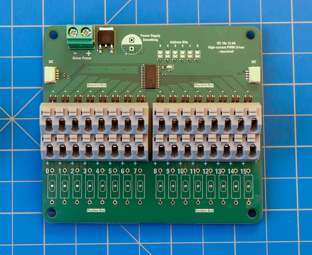
Design
To meet the goals, it was fairly simple to look at some reference designs and get a good idea of the whole project. Adafruit sells a PWM board which I quite like that utilizes NXP’s PCA9685, which is a fairly capable chip. A neat feature that Adafruit doesn’t take advantage of, though, is that the chip is designed around driving LEDs through both N-channel and P-channel MOSFETs, and has that FET driver block built-in. In this case, that’s a huge bonus. From there, it was a simple exercise in reading the datasheet to rough out most of the design. To make it daisy-chainable, I broke out the address pins for it as well.
Finding a MOSFET was trivial, and basically involved finding the cheapest MOSFET with the right Vgs for switching via the PCA9685 and the right Vds(max) for the possible loads. The AO3400A was a good fit, and in stock at most PCBA vendors. Despite being a SOT23 package, it can switch nearly 6A up to 30V, which is almost silly. Its datasheet mentions its design being optimized for PWM, and it can dissapate around 1W of heat.
Basically, the entire design is just marrying these two parts in a nice package, which I still haven’t found online yet. My other major goals were mostly connector-oriented: the places I was installing these (think, indoor holiday decorations) weren’t convenient for soldering, nor did I particularly want permanant connections, so I really wanted good field serviceability. I think I was able to achieve that through the terminal blocks.
Some lights are not as bright as others, and not all decorations need maximum brightness, and I didn’t want to have to rely simply on PWM to cover that gap. Instead, I added a footprint for an optional series resistor that can be used to limit the current for any of the channels. I bridged it out a with a cuttable trace by default, however, and even though that trace probably won’t handle 5A, it can be bridged manually with a wire link.
The input side is the main limiting factor for maximum power output. Each channel can theoretically switch over 5.7A, which at 16 total channels is almost 100A. This board certainly cannot achieve that maximum rating, in no small part due to the power input connector only being rated for around 20A, which I don’t know if I would trust continuously.
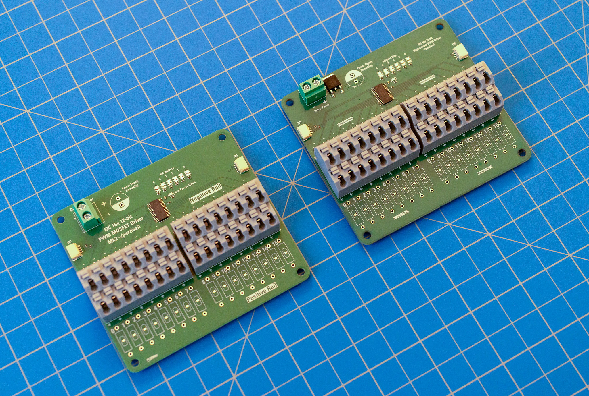
Revisions
Mk. 1
The first revision went a step further for friendliness and had a reverse-polarity protection P-channel MOSFET that would shut off the input power during reverse-polarity events. This unfortunately lowered the maximum power to a measly 8A, which significantly limited the board’s usefulness in larger displays. The maximum power was also limited by the fact that, while the return current path was multiple ground planes on the 4-layer stackup, the current was provided using a single wide bus trace. It worked great for my needs, which only required about 8-10 lights, of which only two or three were ever active at once, but I didn’t think it was very useful to anyone else.
Needless to say, I was not very happy with this design.
Mk. 2
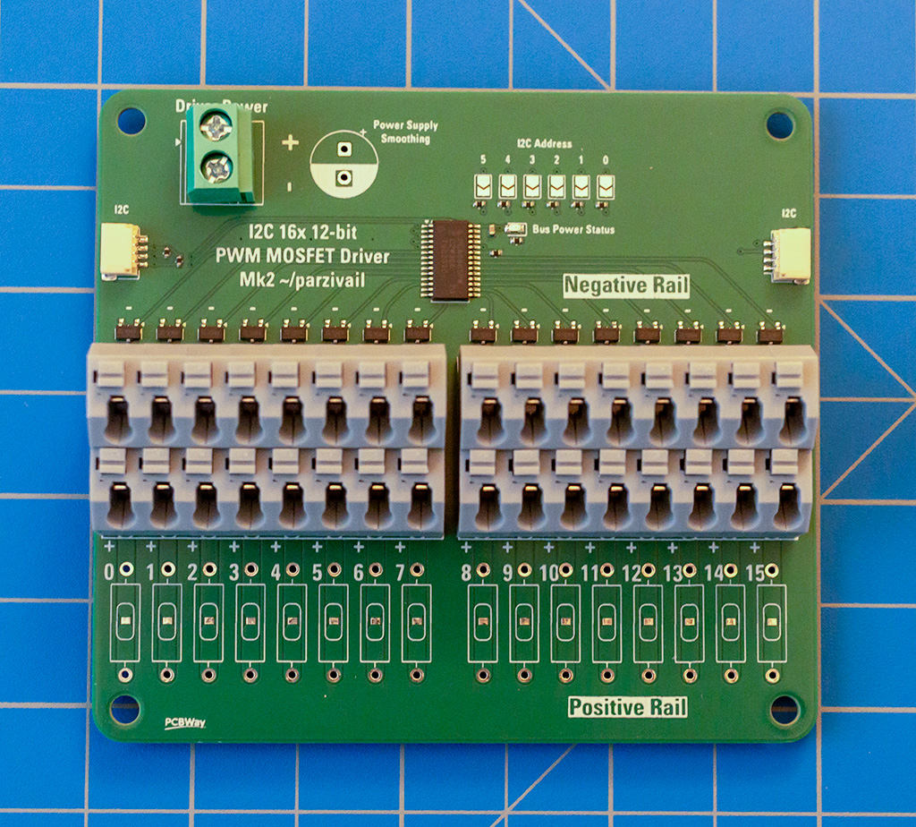
Taking what I learned in practice from Mk. 1, I opted for a small re-design. This time, I ditched the reverse-polarity protection MOSFET and reworked the board stackup to utilize as much copper area as possible for the load power. I moved the connector to be aligned to the incoming I2C cable as well, which made installation easier if I needed to push one board edge up against a wall.
I think with these changes, it can make much better use of the AO3400A’s capacity.
Conclusion
So far, I’ve been pretty happy using these in practice. If anyone else wants to give one a shot, the KiCad project is available on GitHub.
Of course, if you’d like to support this sort of thing (and you’re in the US), you can pick a pre-made one up on Tindie.
Thanks
During the development of this project, PCBWay (referral link) offered to help support manufacturing costs of the Mk. 2 revision. I had not used PCBWay previously, so I was interested to at least try. Compared to the other PCB/PCBA services I have used for other projects, I found it reassuring that people were personally and proactively in contact with me via email in various stages throughout the ordering, manufacturing, and inspection process, and they were able to catch and correct some design mistakes. Additionally, I was able to submit a BOM with links for a third-party parts distributor, and they took care of sourcing those parts, which is very convenient. The lead time for manufacturing this board’s PCB and PCBA, including parts procurement, was 18 days from payment to shipment. The results were of high quality and I’m happy to have them stocked in my store.
If you’re interesting in getting your own PCBs manufactured, kindly consider PCBWay using the referral link above.